Power semiconductor is a kind of microelectronic components that can work under high voltage and high current, and is widely used in various fields such as industry, transportation, medical treatment, home appliances, etc., and the main production process and process of power semiconductor are as follows.
1. Wafer processing
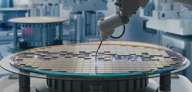
Wafer processing is a fundamental step in the fabrication of power semiconductor devices. Wafers are made of silicon or silicon carbide materials and have a flat surface, and wafer processing includes steps such as cutting, polishing, cleaning, and etching.

Among them, the dicing process is mainly to cut large crystals into small crystals to increase wafer yield. The polishing process is done to remove defects and contaminants from the surface of the wafer and make it more flatter. The cleaning process is to remove chemicals and particulates from the surface. Finally, during the etching process, a chemical liquid is used to corrode the wafer to form the desired structure and pattern.
2. Oxide formation
The oxide layer is an important layer of structure in power semiconductor devices. Its main role is to provide electrical insulation and prevent oxidation of the material.

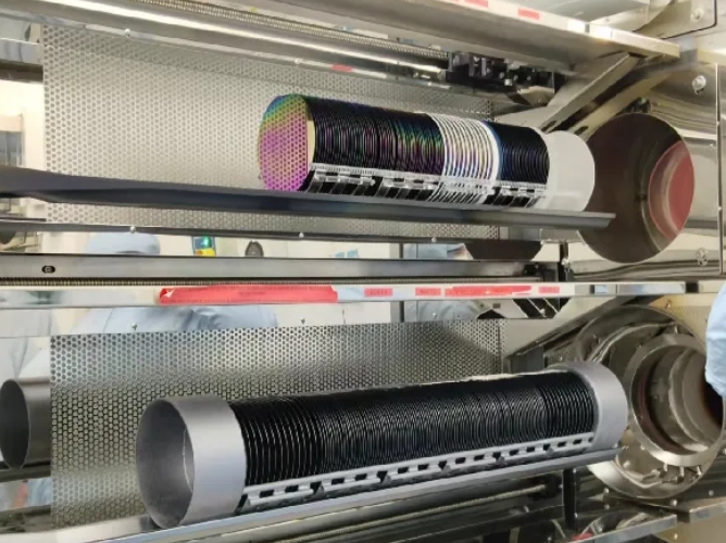
During the manufacturing process, an oxide layer is first formed on the surface of the wafer. In general, the wafer is exposed to the high temperature of an oxidation furnace and injected with silane (SiH₄) and oxygen to react on the surface of the wafer to form silicon dioxide (SiO₂).
3. Physical vapor deposition
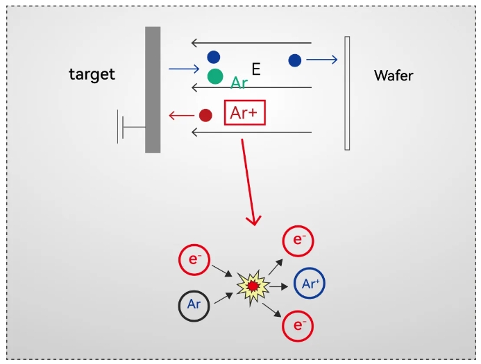
Physical vapor deposition (PVD) is the process of depositing thin films on the surface of a wafer using plasma technology. It uses phenomena such as the sputtering of atoms on the surface of a substance when bombarded by a particle beam, so as to achieve a controlled transfer from the source material (target) to the product chip.

This process is mainly used for the deposition of SCHOTT-metal, front-side metal, and back-side metal. Sputter deposition can use a variety of materials such as metals, alumina, etc.
4. Lithography process
The photolithography process is a microelectronic manufacturing process that uses photosensitive adhesive film as the pattern transfer medium. The basic principle is to use light to portray the photosensitive film into the desired pattern, and then use this pattern as an etching mask to etch the pattern on a silicon or silicon carbide substrate.

5. Ion implantation
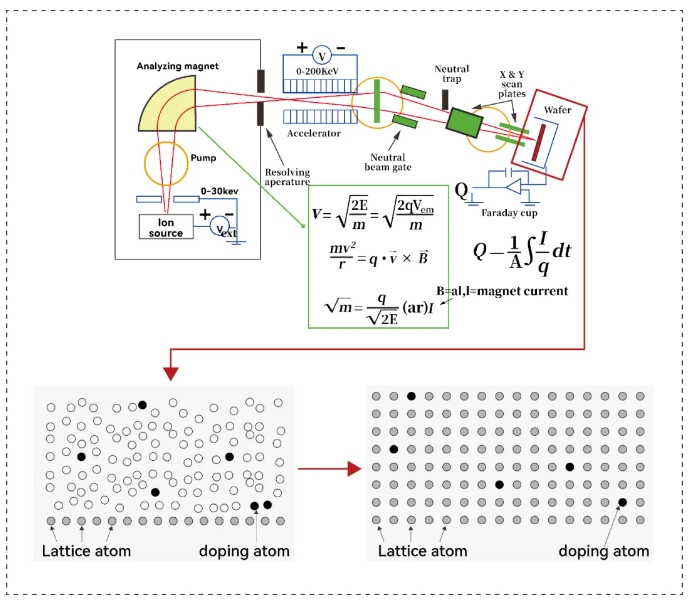
Ion implantation is one of the main processes of integrated circuit manufacturing, which changes the physical properties of the surface of the material by accelerating the ion beam to a certain energy range (generally on the order of keV) and then injecting it into the surface layer of a solid material. In integrated circuit processes, the solid material is usually silicon or silicon carbide. The mainstream process chooses aluminum (AL) as P-type doping and nitrogen (N) as N-type doping.

After ion implantation, the pieces are placed in a high-temperature activation furnace and activated at a process temperature of 1700°C to repair lattice damage.
6. Metallization and encapsulation
Metallization and packaging are the last two process steps in the fabrication of power semiconductor devices. Front-side metallization refers to the coating of a metal film on the surface of the chip to form the positive electrode of the diode, which is generally more than 4 μm. Titanium and nickel are generally selected as the three layers of back metal for back metallization, mainly to increase the flexibility of the component and reduce the thermal impedance of the chip to further improve the performance, and the thickness is within 10μm. Subsequently, the components will be encapsulated in the appropriate enclosure to ensure the reliability and stability of the device.
Related information
-
Wechat

-
Phone
18928454078 -
Tiktok

